
NVIDIA GeForce RTX 5000 Blackwell Brings GDDR7 Up to 32 Gbps, DisplayPort 2.1 4K240, and Up to 120% Ray‑Tracing Gains
With consumer SKUs still unannounced, standards milestones, data‑center Blackwell disclosures, and converging reports outline a 2025–2026 GeForce generation with 1.34–1.54 TB/s bandwidth, next‑gen Tensor/RT cores, and safer 12V‑2x6 power
NVIDIA’s next GeForce chapter is taking shape around three concrete pillars: faster GDDR7 memory, a long‑awaited jump to DisplayPort 2.1 for uncompressed 4K240, and an architectural cadence that prioritizes Tensor throughput, ray‑tracing efficiency, and tighter scheduling. While NVIDIA hasn’t announced consumer Blackwell SKUs as of February 10, 2026, the signals are consistent. Standards are locked. Data‑center Blackwell is out in the open. And third‑party reporting continues to coalesce around a 2025–2026 GeForce rollout that pairs 33–53% more memory bandwidth with next‑gen RT/Tensor cores and a safer, broadly adopted 12V‑2x6 power connector.
For enthusiasts aiming at 4K high‑refresh gaming, the upshot is straightforward: a flagship “5090‑class” card is tracking to roughly 30–60% higher 4K raster performance than RTX 4090, and 50–120% gains in heavy ray‑traced workloads once new RT core machinery and DLSS denoising improvements are factored in. Creator pipelines and local AI inference stand to gain 1.5–3× depending on precision and software maturity. Many details remain unannounced, but the trajectory is clear—and it’s meaningful for both desktops and laptops rolling through 2025 and into 2026.
The line between official and inferred: where things stand today
What’s official today lives in NVIDIA’s Blackwell platform unveil for data centers: low‑precision formats like FP8/FP4, a second‑generation Transformer Engine, higher interconnect bandwidth, and scheduling refinements that push training and inference throughput beyond Hopper. Those are enterprise disclosures, not gaming SKUs, but historically they foreshadow how GeForce generations evolve—especially in Tensor hardware, memory subsystem emphasis, and scheduler behavior.
On the standards side, the groundwork for consumer Blackwell is firm. JEDEC has published the GDDR7 standard, and memory vendors have announced 28–32 Gbps devices, unlocking a substantial bandwidth increase without widening buses. VESA’s DisplayPort 2.1 is also finalized, with UHBR link rates up to 80 Gbps raw (~77.4 Gbps effective), which finally enables uncompressed 4K240 10‑bit 4:4:4. Meanwhile, PCI‑SIG’s 12V‑2x6 auxiliary connector—the safer successor to 12VHPWR—has been ratified and is propagating across new PSUs and board designs.
Consumer specifics—die sizes, SM counts, clock targets, SKUs, prices—remain undisclosed. Performance expectations and power ranges referenced here are projections grounded in the standards, in past NVIDIA behavior, and in cross‑checked reporting; they are best treated as evidence‑based scenarios rather than firm commitments.
GDDR7 and DisplayPort 2.1: the bandwidth and display leap
The most tangible leap for GeForce Blackwell is in memory bandwidth. With GDDR7 at 28–32 Gbps per pin:
- A 384‑bit flagship at 28 Gbps delivers roughly 1.34 TB/s.
- At 32 Gbps, that rises to about 1.54 TB/s.
- Upper‑mid designs on a 256‑bit bus at those speeds reach ~0.90–1.02 TB/s.
For context, RTX 4090’s 24 GB of 21 Gbps GDDR6X on a 384‑bit bus yields ~1,008 GB/s. Even holding bus width constant, a 33–53% increase in effective bandwidth directly relieves contention in 4K raster, texture‑heavy scenes, real‑time path tracing, and AI denoising—precisely the mixture that defines today’s top‑end gaming workloads.
On the display side, DisplayPort 2.1 is the linchpin. With UHBR10/13.5/20 rates and 128b/132b encoding, DP 2.1 provides up to ~77.4 Gbps effective throughput—enough for uncompressed 4K240 10‑bit 4:4:4 and far more headroom for high‑refresh 5K/6K or multi‑monitor arrays without leaning on DSC. AMD shipped DP 2.1 in RDNA 3; it’s widely expected the next NVIDIA generation matches that capability, though consumer confirmation is still pending. HDMI 2.1’s 48 Gbps FRL remains standard for TVs and AVRs.
The combination of GDDR7 bandwidth and DP 2.1 display plumbing is decisive for the next few years of PC gaming: higher native refresh targets at 4K without compression compromises, and fewer bottlenecks for advanced lighting techniques and AI‑assisted reconstruction.
Architectural direction: SMs, RT and Tensor cores, and smarter scheduling
While NVIDIA hasn’t detailed consumer Blackwell microarchitecture, the directional moves are visible:
- More SM throughput and smarter scheduling: Expect higher SM counts per flagship die, refined dual‑issue or warp scheduling behavior, and more L1/shared memory per SM to improve throughput per clock. A larger L2 cache footprint is a logical extension of Ada, reducing trips to external memory—especially valuable for irregular locality in ray‑traced and AI‑denoised scenes.
- Next‑gen RT cores: A fourth‑generation RT block with faster BVH traversal, higher triangle/box intersection rates, and tighter integration with Shader Execution Reordering would push larger real‑world gains in path‑traced and heavy‑RT titles than pure raster. Expanded hardware acceleration for RT‑friendly data structures—such as micro‑meshes or opacity micromaps—would further reduce shader pressure.
- Fifth‑gen Tensor cores: Consumer exposure of FP8 (and potentially FP4) along with better sparsity support would raise the ceiling for super‑resolution and denoising models, reduce artifacts in Frame Generation, and accelerate local AI inference. Exact formats and throughput in GeForce drivers may differ from data‑center products, but the trajectory aligns.
- Display/media pipeline: DisplayPort 2.1 UHBR should land with consumer Blackwell boards, and NVIDIA’s media engines typically gain per‑stream throughput each generation. AV1 encode/decode is already baseline on Ada; AV2 hardware support remains unconfirmed as of today.
- Interconnects: PCIe 4.0 x16 has been sufficient for gaming; a move to PCIe 5.0 x16 is possible but would deliver negligible real‑world gains in single‑GPU play. Consumer NVLink is not expected to return.
None of these shifts are exotic. They extend the same priorities that made Ada excel: caching more, stalling less, and overlapping Tensor, RT, and shader work with tighter scheduling.
Projected performance: raster, ray tracing, and AI
Projected flagship uplift versus RTX 4090 clusters around three bands:
- Rasterization: About 30–60% at 4K, driven by GDDR7 bandwidth, more SM resources, and incremental clocks. At 1440p, expect 20–45%; at 1080p, 10–35% as CPU limitations bite.
- Ray tracing: Approximately 50–120% in heavy‑RT configurations at 4K, with the top end contingent on improved RT core microarchitecture plus better denoising (e.g., DLSS Ray Reconstruction and likely successors). Pure hardware RT microbenchmarks would tend toward the lower half of the range.
- AI and inference: Roughly 1.5–3× for local generative AI and inference tasks, helped by low‑precision formats and fatter Tensor pipes, alongside higher effective memory bandwidth.
Mid‑stack expectations align accordingly:
- An “upper‑mid” 5080‑class device: Approximately 20–40% more 4K raster than RTX 4080 Super, with 35–80% in heavy‑RT scenarios depending on software integration.
- A “5070‑class” device: About 15–30% over 4070 Ti Super at 1440p/4K.
DLSS 3.5’s Ray Reconstruction is already a big swing factor in RT‑heavy games. A successor iteration—often referenced colloquially as “DLSS 4,” though unannounced—would be expected to capitalize on stronger Tensor cores and improved optical‑flow to deliver higher perceived FPS with reduced artifacts and tighter latency. The realized gains will continue to hinge on game‑level integrations and Reflex pipelines as much as on raw silicon upgrades.
Quick bandwidth math
| Configuration | Bus width | Per‑pin speed | Effective bandwidth |
|---|---|---|---|
| RTX 4090 (Ada) | 384‑bit | 21 Gbps (GDDR6X) | ~1,008 GB/s |
| Flagship candidate | 384‑bit | 28 Gbps (GDDR7) | ~1.34 TB/s |
| Flagship candidate | 384‑bit | 32 Gbps (GDDR7) | ~1.54 TB/s |
| Upper‑mid candidate | 256‑bit | 28–32 Gbps (GDDR7) | ~0.90–1.02 TB/s |
Specific die sizes, clocks, and transistor counts remain undisclosed.
Power, thermals, and platform readiness
Expect top‑end total board power to land in a familiar but formidable range: roughly 450–600 W for a flagship, with mid‑stack parts clustering around 220–400 W. AIB coolers will continue trending toward 3–4‑slot designs, large vapor chambers, and higher static‑pressure fan profiles tuned for transient load handling and acoustics.
Just as importantly, the ecosystem is standardizing on the 12V‑2x6 power connector. It supersedes 12VHPWR with stricter mechanical/electrical tolerances while maintaining platform compatibility. For builders, high‑quality ATX 3.x PSUs with native 12V‑2x6 cables simplify cabling and improve transient robustness.
Practical PSU guidance by tier:
- Flagship builds: 1000–1200 W for overclocking headroom and high‑power CPUs; 850–1000 W for efficient, stock‑clocked configurations.
- Upper‑mid builds: 850–1000 W, depending on CPU and peripherals.
- Mainstream (220–300 W GPUs): 650–850 W modern, high‑efficiency units.
These recommendations assume contemporary PSUs with strong transient response and appropriate protections; legacy units with similar nameplate wattage may not behave equivalently.
Software stack and creator impact
NVIDIA’s current software baseline sets the stage for outsized perceived gains:
- DLSS 3.5 with Ray Reconstruction already lifts image stability and lighting reconstruction in RT‑heavy scenes, independently of Frame Generation.
- RTX Video Super Resolution improves streaming/video upscaling quality across browsers and player apps.
- NVENC/NVDEC support already includes AV1 encode/decode on Ada; a next‑gen media engine would reasonably add per‑stream throughput and quality headroom. AV2 hardware acceleration is unconfirmed.
For creators, the expected hardware moves translate into real time:
- GPU rendering (Blender/Cycles, Octane, V‑Ray): Typically scales with bandwidth and denoiser performance; a 30–70% uplift versus RTX 4090 is plausible at the flagship tier.
- Video pipelines: NVENC/NVDEC throughput improvements in the 20–50% per‑stream range would benefit multi‑stream AV1 production and live encoding.
- AI‑accelerated effects (Premiere Pro, DaVinci Resolve, and similar): Often see 1.3–2× speedups tied to Tensor performance and memory bandwidth.
- Local generative AI (Stable Diffusion image/video, LLM inference): Expect 1.5–3× acceleration driven by FP8/INT8 paths in frameworks such as TensorRT‑LLM, plus higher effective bandwidth. Larger VRAM options at the top end enable bigger batch sizes or longer context windows.
As always, software maturity and integration matter. Gains arrive fastest where engines embrace DLSS Ray Reconstruction (and successors), SER, mesh shading, and optimized batching.
Competition and market positioning
Competitive signals suggest NVIDIA will remain out front in ray tracing and AI features at the top end. Reporting through late‑2025 and early‑2026 points to AMD’s RDNA 4 focus on the midrange with uncertain halo presence and to Intel’s Battlemage targeting upper‑mid raster tiers rather than true flagship contention. Raster leadership at 4K is likely for NVIDIA’s top GeForce Blackwell SKU, though specific price/perf bands could be contested depending on RDNA 5 timing, bus widths, and GDDR7 penetration across stacks.
Confidence in these competitive projections is medium to low until rival launches finalize, but the directional takeaway is consistent: ray‑traced performance and AI‑assisted rendering remain NVIDIA’s strongest moats at the premium tier.
Mobile vs. desktop: staggered rollouts and real‑world constraints
Desktop typically moves first at the high end, with Founders Edition and partner boards spanning triple‑fan to ultra‑thick quad‑slot coolers. Expect VRAM in the 16–32 GB range from upper‑mid to flagship classes depending on bus widths and memory densities. Full DisplayPort 2.1 bandwidth is most consistently realized on desktops with direct GPU‑attached ports.
Laptops follow in waves:
- Thin‑and‑light designs around 35–80 W.
- Performance notebooks from ~80 W up to 175 W or more.
Mobile parts usually deploy smaller dies and lean on binning, aggressive power‑gating, and smart boost behavior. Real‑world performance generally lands at 50–80% of desktop analogs at like‑for‑like SKU names due to tighter power budgets. DisplayPort 2.1 features depend on platform wiring and panel choices: many notebooks route through the iGPU or use eDP panels, which can limit exposure to desktop‑class DP 2.1 outputs.
Pricing scenarios, release windows, and what to watch next
Timelines remain unannounced, but a plausible cadence is high‑end consumer Blackwell in 2025, with broader stack coverage through 2026. Pricing scenarios—sensitive to wafer costs, yield, inventory digestion, and competitive pressure—map roughly to familiar Ada‑era tiers:
- “5090‑class” flagship: $1,599–$1,999
- “5080‑class” upper‑mid: $999–$1,199
- “5070 Ti/Super‑class” enthusiast‑mid: $599–$799
- Mid‑mainstream: $399–$599
Early flagship availability often starts tight, improving over subsequent months. Regional pricing will vary by taxes, tariffs, and logistics. Treat these figures as placeholders pending official announcements.
Key markers to track next:
- Confirmation of bus widths and memory capacities across the stack.
- DisplayPort 2.1 UHBR support details for both desktop and laptop designs.
- Media engine disclosures (per‑stream throughput; any AV2 hardware signal).
- PCIe versioning on consumer dies (4.0 vs. 5.0) and any package interconnect tweaks.
- Power targets and cooling designs from AIBs, including broad adoption of 12V‑2x6.
- Software updates around DLSS Ray Reconstruction successors and TensorRT‑LLM optimizations for FP8/INT8 pathways.
Bottom line
Blackwell‑based GeForce looks set to raise the ceiling for 4K gaming and creator workflows in ways that matter day‑to‑day: GDDR7 memory pushes effective bandwidth into the 1.34–1.54 TB/s range for a 384‑bit flagship, DisplayPort 2.1 removes the last big friction for uncompressed 4K240, and next‑gen RT/Tensor cores should convert silicon progress into bigger real‑world wins for path tracing and AI‑assisted rendering than raster alone.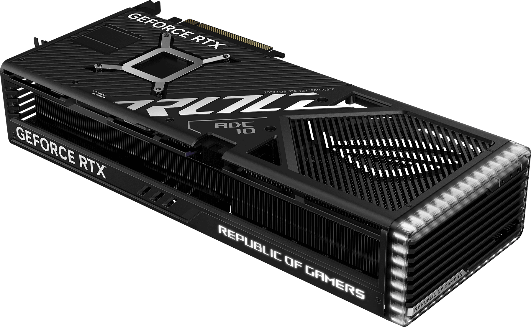
A black NVIDIA GeForce RTX 4090 graphics card with a sleek design, large cooling vents, and prominent branding, featuring a transparent LED strip on one edge.
On paper, a 30–60% raster uplift and 50–120% gains in heavy RT over RTX 4090 are within reach at the top end, while AI workflows and media pipelines stand to leap 1.5–3× depending on format exposure and SDK maturity. Power envelopes remain stout, but the shift to 12V‑2x6 and a mature ATX 3.x PSU ecosystem improves build safety and simplicity. Competitive dynamics could tighten select bands, yet NVIDIA’s lead in ray tracing and AI‑assisted features remains the defining story heading into 2026.
For builders, the guidance is pragmatic: plan for DP 2.1 displays if you care about 4K240 without DSC, size PSUs with transient headroom in mind, and watch for early AIB designs that lean into vapor chambers and thicker radiators. For gamers and creators, the promise is equally pragmatic—faster frames, steadier pacing under heavy RT, and quicker turnarounds on renders and AI tasks. The exact SKUs and prices will decide the value calculus, but the direction of travel is unmistakable. 🚀