CoWoS‑L and Dual‑Node GPU Design Lift 2026 Throughput
The most consequential accelerators of 2026 won’t win on core count alone—they’ll win on how fast they can be built. Two facts set the stage. First, advanced packaging and HBM attach, not lithography, dominate door‑to‑door cycle time for AI GPUs. Second, TSMC’s customers are shifting from full interposers to CoWoS‑L’s localized bridges and selectively adopting SoIC, raising effective line throughput. Paired with a pragmatic dual‑node design that keeps reticle‑scale compute tiles on N4/4N and migrates select chiplets to N3, these changes collectively pull module lead times toward roughly 80–120 days in 2026 and lift packaged output.
This matters now because the bottlenecks have moved. CoWoS capacity doubled in 2025 and continues to expand across multiple 3DFabric sites, while 12‑high HBM3E grows across all three top suppliers but remains tight at the fastest speed bins. Nvidia‑class GPU floorplans that embrace CoWoS‑L and targeted chiplet partitioning are best positioned to exploit the new balance.
This article dissects the architecture and manufacturing choices behind that outcome. We’ll detail why N4/4N remains the economic sweet spot for reticle‑scale dies in 2026, where N3E/N3P chiplets make sense, how CoWoS‑S/L/R and SoIC change interposer area and wiring, what ABF mega‑substrates still constrain, how EUV contributes (and where it doesn’t), the 80–120‑day cycle‑time math, and how 12‑high HBM3E attach and MR‑MUF steer thermal and warpage control. Readers will leave with a concise set of best‑practice patterns tuned for throughput without giving up PPA. 🧩
Architecture/Implementation Details
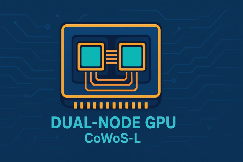
Dual‑node partitioning: N4/4N for reticle‑scale compute, N3 for targeted chiplets
In 2026, the physics and economics remain uncompromising: very large, reticle‑scale compute tiles are highly yield‑sensitive and still pencil out best on N4/4N. Meanwhile, selective chiplets—such as I/O, control, PHYs, and similar medium/small logic—can migrate to N3E/N3P to harvest power and area improvements without blowing out package cost.
TSMC confirms the N3 family is in broad ramp, while N2 entered high‑volume manufacturing in 4Q25, with N2P and A16 following in 2H26. N2 targets roughly a 10–15% speed uplift at the same power or a 25–30% power reduction at the same speed over N3E, plus 15%+ logic density; A16 adds another 8–10% speed or 15–20% power reduction and 7–10% density versus N2P. Even with these gains, the most pragmatic 2026 mix keeps the majority of reticle‑scale compute tiles on N4/4N, with approximately 10–30% of accelerator‑adjacent wafer starts on the N3 family for smaller chiplets. Early N2 usage concentrates on smaller logic elements rather than wholesale migration of massive GPU compute tiles.
Bottom line: a split‑node approach maximizes usable die per wafer where it counts (compute) and pulls forward PPA where it fits (I/O, controllers), without inflating package risk.
CoWoS variants: S vs L vs R—reclaiming interposer area and line time
- CoWoS‑S (full silicon interposers) set the baseline for large multi‑die AI packages but consume large interposer area and TSV‑intensive capacity.
- CoWoS‑L introduces localized silicon bridges that preserve high‑bandwidth die‑to‑die connectivity while materially shrinking full‑interposer area. This shift improves effective throughput per square meter and alleviates some capacity constraints tied to very large interposers.
- CoWoS‑R employs reconstituted wafer flows, broadening manufacturable configurations and offering additional assembly flexibility.
Customers are transitioning from CoWoS‑S to CoWoS‑L, a change that pairs neatly with chiplet partitioning. By reducing total interposer real estate and simplifying aspects of the assembly flow, CoWoS‑L shortens packaging queues—the single biggest contributor to door‑to‑door cycle time for accelerators.
Selective SoIC stacks: wiring length, bump density, and substrate relief
SoIC hybrid bonding, offered face‑to‑face and face‑to‑back, enables logic‑on‑logic and memory‑adjacent logic stacks that materially elevate bump density and shorten interconnect length. The practical payoff is twofold: lower latency between tightly coupled functions and partial relief of routing pressure on the interposer and ABF substrate. As designs adopt N3E/N3P chiplets for controllers or cache‑adjacent logic, SoIC becomes a clean way to integrate without expanding the interposer footprint.
Specific bump‑pitch metrics are not disclosed, but the direction is clear: hybrid bonding compresses critical wiring while maintaining high‑bandwidth connectivity in spaces where bumps, vias, and traces were previously capacity‑intensive.
ABF mega‑substrates: the quiet gate on the biggest packages
Even as CoWoS scales, ABF mega‑substrates—very large panels with high layer counts and fine line/space—remain a limiting factor, particularly for top‑end GPU modules. Suppliers are investing, but credible industry reporting points to 2026 capacity at some houses already substantially pre‑booked by large technology buyers. Unimicron has redirected capacity toward CoWoS‑class demand and ramped new AI GPU substrate lines, reinforcing how critical this layer of the stack has become.
Quantitatively, lead times for the largest ABF formats are easing toward roughly 12–20 weeks in 2026, but tightness persists at the very high end. Specific line/space, layer‑count, and warpage tolerance metrics remain undisclosed, yet yield stressors scale with size and complexity; any floorplan that reduces interposer area and routing congestion directly helps substrate manufacturability and throughput.
EUV’s role: helpful, not decisive
ASML’s NXE:3800E lifts wafers‑per‑hour and availability for EUV layers, providing incremental wafer‑side relief at N3/N2 and marginally trimming fab cycle time. For AI accelerators, however, the wafer contribution is not the bottleneck. The dominant lever remains advanced packaging and HBM attach. EUV gains matter—but they do not change the reality that package assembly queues drive the calendar.
Cycle‑time math: 80–120 days door‑to‑door in 2026
In 2025, typical door‑to‑door cycle time for Nvidia‑class accelerators ran about 90–140 days. With CoWoS expansion (including a capacity doubling in 2025) and the industry’s shift toward CoWoS‑L and SoIC, 2026 trends toward roughly 80–120 days. Within that envelope:
- Packaging cycle time is trending near approximately 6–10+ weeks, depending on configuration and rework loops.
- HBM attach and underfill remain variable, particularly at the 12‑high stacks that stress thermal and warpage controls.
- Wafer‑side improvements help at the margins, but they are not the pacing item for modules.
Lead times for HBM and ABF also shape how quickly finished modules can ship. In the base case, HBM lead times ease toward roughly 12–20 weeks in 2026, with fastest 12‑high speed bins still the scarcest. ABF mega‑substrates track a similar 12–20 week range, but availability for the largest, highest layer‑count formats remains tight.
12‑high HBM3E attach: MR‑MUF, thermals, warpage, and rework containment
The industry’s move to 12‑high HBM3E amplifies assembly risk and thermal flux. SK hynix and Samsung both tout mass production of 12‑layer HBM3E, while Micron’s production‑capable 12‑high HBM3E exceeds 1.2 TB/s with pin speeds above 9.2 Gb/s—and Micron notes its entire 2026 HBM supply (including early HBM4) is fully committed. These stacks demand careful attach and underfill: warpage during cure, CTE mismatch, and localized heat flux raise rework probabilities.
Advanced MR‑MUF (molded underfill) specifically targets these stressors. SK hynix highlights improved warpage control and thermal dissipation with its Advanced MR‑MUF process, which helps keep assemblies within co‑planarity and reliability windows during and after cure. On the line, MR‑MUF contributes to lower rework, more predictable queues, and better module‑level thermal stability—vital as packages push toward the upper envelope of HBM speed bins.
Floorplanning tuned for CoWoS‑L
Design teams increasingly shape floorplans to minimize full‑interposer spans and route the highest‑bandwidth links across localized bridges. This CoWoS‑L‑aware placement reduces total interposer area and alleviates substrate routing pressure. The approach pairs naturally with selective SoIC for short‑reach logic stacks. Specific placement rules and bridge counts are design‑dependent, and detailed metrics are not disclosed, but the pattern is consistent: shrink the silicon footprint that consumes TSV and litho capacity, keep critical links short and local, and reserve substrate layers for long‑reach routes that do not require fine‑pitch silicon wiring.
Test strategy and known‑good‑die (KGD): aligning to 3DFabric throughput
As TSMC scales advanced packaging and test across multiple 3DFabric sites in Taiwan, test capacity alignment becomes a practical gating item. Successful teams raise KGD thresholds before assembly, maintain partial rework loops for HBM and component swap where feasible, and dual‑qualify programs across sites to avoid bottlenecks. Specific KGD metrics remain undisclosed, but the operational thrust is clear: shift defect discovery earlier, reduce full‑module scrap, and synchronize final test availability with packaging output to avoid idle WIP.
Comparison Tables
CoWoS variants and integration choices
| Technology | What it is | Throughput/area impact | Where it helps most |
|---|---|---|---|
| CoWoS‑S | Full silicon interposer | Largest interposer area; TSV intensive | Early large AI packages; maximum flexibility at cost of area |
| CoWoS‑L | Localized silicon bridges | Reduces full‑interposer area; raises effective module throughput | High‑bandwidth chiplet‑to‑compute links with smaller silicon footprint |
| CoWoS‑R | Reconstituted wafer flows | Broadens manufacturable configurations; assembly flexibility | Complex multi‑die layouts and alternative assembly routes |
| SoIC (hybrid bonding) | Face‑to‑face/back logic stacking | Higher bump density; shorter wiring; substrate/interposer relief | Logic‑on‑logic, cache‑adjacent logic, memory‑adjacent control |
Node choice for 2026 accelerators
| Node family | 2026 role | Rationale | Notes |
|---|---|---|---|
| N4/4N | Primary for reticle‑scale compute tiles | Yield/cost for very large dies | Anchor for performance without undue cost risk |
| N3E/N3P | Select chiplets (I/O, PHYs, controllers) | Power/area gains without large‑die yield penalties | ~10–30% of accelerator‑adjacent wafer starts |
| N2/N2P/A16 | Limited 2026 use, smaller logic | PPA gains strong, but early ramp and economics for big tiles | Broader adoption more plausible late‑2026/2027 |
Cycle‑time and supply contributors in 2026
| Contributor | Typical 2026 effect | Quantitative notes |
|---|---|---|
| Advanced packaging (CoWoS line) | Largest share of door‑to‑door time | Packaging cycle trending ~6–10+ weeks |
| Door‑to‑door module cycle | Overall calendar | ~80–120 days for accelerators |
| HBM supply and attach | Co‑bottleneck with packaging | HBM lead times easing to ~12–20 weeks; fastest 12‑high bins tight |
| ABF mega‑substrates | Gate for largest packages | Lead times trending ~12–20 weeks; some 2026 capacity pre‑booked |
| EUV wafer‑side | Incremental relief | NXE:3800E boosts throughput but not the pacing item |
Best Practices
1) Keep compute massive—and on N4/4N in 2026
- Anchor reticle‑scale compute tiles on N4/4N for yield and cost predictability.
- Pull targeted PPA gains by moving medium/small chiplets (I/O, controllers, PHYs) to N3E/N3P.
- Reserve N2/N2P/A16 for carefully scoped smaller logic pilots in 2026.
2) Design for CoWoS‑L first, CoWoS‑R second
- Floorplan to minimize full‑interposer area; place highest‑bandwidth links across localized bridges.
- Use CoWoS‑R when reconstituted flows or nonstandard die shapes/configurations lift assembly yield or availability.
- Expect better line throughput as CoWoS‑L adoption rises across 3DFabric sites.
3) Deploy selective SoIC to shorten critical paths
- Stack cache‑adjacent or control logic via SoIC to raise bump density and cut wire length.
- Offload dense short‑reach links from the interposer and ABF substrate to reduce routing congestion.
- Maintain thermal budgeting for stacked logic; specific derating metrics unavailable, so validate early.
4) Engineer for ABF realities
- Choose package configurations that avoid the very largest, highest layer‑count ABF formats when feasible.
- Use CoWoS‑L to shrink the total silicon/interposer footprint, easing substrate routing complexity.
- Anticipate ABF lead times around 12–20 weeks; design alternate substrate options where practical.
5) Tame 12‑high HBM3E attach with MR‑MUF‑aware flows
- Align assembly to Advanced MR‑MUF to control warpage and improve thermal dissipation on 12‑high stacks.
- Expect variability at top speed bins; plan partial rework loops to avoid scrapping full modules.
- Multi‑source 12‑high HBM speed bins to absorb supplier‑specific yield swings.
6) Synchronize KGD and test with packaging throughput
- Push KGD thresholds earlier in the flow; specific thresholds unavailable, but aim to cut module‑level scrap.
- Dual‑qualify test programs across multiple TSMC 3DFabric sites to keep final test off the critical path.
- Maintain known‑good HBM and substrate buffers sized to typical assembly recovery tempos.
Conclusion
The architecture and manufacturing winners of 2026 will be the teams that treat CoWoS‑L, selective SoIC, and dual‑node partitioning as a single system. Keeping reticle‑scale compute on N4/4N while shifting targeted chiplets to N3E/N3P aligns with yield economics and unlocks power/area in the right places. CoWoS‑L’s localized bridges shrink interposer area and elevate line throughput; SoIC shortens critical wiring and relieves substrate pressure. EUV improvements help, but packaging and HBM attach remain the pacing items. With ABF mega‑substrates still tight at the largest formats and 12‑high HBM3E top bins scarce, the practical path to throughput is clear: design to reduce full‑interposer area, favor short‑reach stacked logic, and synchronize KGD and test with packaging capacity.
Key takeaways:
- Keep compute tiles on N4/4N in 2026; move select chiplets to N3E/N3P.
- Prefer CoWoS‑L to reduce interposer area and lift effective line throughput.
- Use SoIC to compress critical interconnects and ease substrate routing.
- Expect ~80–120 day door‑to‑door cycles; packaging and HBM attach dominate.
- Manage 12‑high HBM3E with MR‑MUF‑aware flows and partial rework loops.
Actionable next steps:
- Re‑partition floorplans around CoWoS‑L bridges; validate signal‑path timing on localized links.
- Define N3 chiplet candidates and SoIC stack pairs with the largest wiring/latency payoffs.
- Lock ABF and HBM options that avoid the most constrained formats and speed bins; build alternate SKUs.
- Align KGD/test plans with multi‑site 3DFabric capacity and establish rework containment triggers.
Looking ahead, as N2P and A16 mature and CoWoS‑L/R plus SoIC reach broader operational tempo across TSMC’s sites, the next wave of GPU modules can further compress queues. But in 2026, the throughput edge belongs to designs that minimize silicon interposer footprint, stack the right logic, and treat packaging as the central performance path. 🛠️