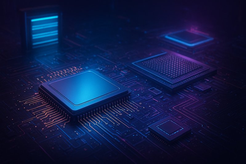
Backside Power and Hybrid Bonding Reshape the 2027 AI Stack
N2P/A16, SoIC, HBM4, and panel‑level packaging mark the next design inflection beyond today’s CoWoS‑centric era
The last two years proved that packaging, not just lithography, sets the pace for AI accelerators. With CoWoS capacity doubling in 2025 and more balance expected in 2026, the bottleneck is shifting from “can we assemble it?” to “how do we assemble smarter?” That pivot coincides with a new wave of silicon changes: N2’s high‑volume manufacturing start in 4Q25, the arrival of backside power at N2P and A16 in 2H26, and the first meaningful hybrid‑bonded stacks for logic‑on‑logic using SoIC. On the memory front, HBM4’s 2Q26 ramp and 12‑high HBM3E maturity raise bandwidth ceilings—but complicate integration and supply dynamics.
This article maps the near‑term innovation arc through 2027: what N2/N2P/A16 actually deliver in speed, power, and density; how backside power and SoIC hybrid bonding rewire die‑to‑die hierarchies; where CoWoS‑L/R and reconstituted flows expand the design space; what HBM4 above 11 Gb/s unlocks and still constrains; and how panel‑level packaging and U.S. qualification steps could change throughput. Readers will leave with a clear view of the technologies that matter, the timelines to watch, and the leading indicators that will separate signal from noise in the next AI accelerator cycle. 🧠
Research Breakthroughs
N2 to A16: quantifiable deltas and the role of backside power
TSMC’s N2 entered high‑volume manufacturing in 4Q25, tracking ahead of prior leading nodes on defect density and positioned for a faster ramp in 2026. The measured deltas versus N3E are crisp: 10–15% higher speed at the same power or 25–30% lower power at the same speed, alongside more than 15% logic density gain. That immediate efficiency lift supports early adoption in smaller logic elements and mobile SoCs, while yield and cost dynamics keep reticle‑scale compute largely on N4/4N through 2026.
Backside power delivery arrives with N2P and A16, both targeted for high‑volume windows in 2H26. A16 layers additional gains over N2P—another 8–10% speed or 15–20% power reduction, plus a further 7–10% density increase. The design implication is straightforward: in 2026 and into 2027, backside power becomes a power‑integrity and IR‑drop lever that frees more front‑side routing for signal, enabling either higher clocks at constrained voltages or deeper power savings at a fixed performance point.
Summary of node‑level improvements:
| Node comparison | Speed uplift (same power) | Power reduction (same speed) | Density gain |
|---|---|---|---|
| N2 vs N3E | 10–15% | 25–30% | >15% |
| A16 vs N2P | 8–10% | 15–20% | 7–10% |
Specific compiler or workload‑level benchmarks are unavailable, but these physical‑design‑level metrics set clear targets for EDA and floorplanning teams to translate into system‑level efficiency gains.
SoIC hybrid bonding: face‑to‑face and face‑to‑back logic stacks
Hybrid bonding moves beyond micro‑bumps. SoIC supports face‑to‑face (F2F) and face‑to‑back (F2B) die stacking for logic‑on‑logic and memory‑on‑logic, tightening interconnect pitch, reducing parasitics, and reclaiming precious package and interposer routing. In AI accelerators, SoIC’s near‑monolithic interconnect density enables:
- Compact cache‑adjacent stacks without long interposer traces
- Tight coupling between control/I‑O logic and compute clusters
- Pathways to split “monolithic” functions across stacked tiers while keeping latency low
Customers are already adopting SoIC in AI/data center contexts, and its integration alongside CoWoS variants broadens architectures beyond today’s planar, full‑interposer mindset.
CoWoS evolves: localized bridges, reconstituted flows, and shrinking interposer footprints
CoWoS‑S established the template for large, multi‑die AI modules on a full silicon interposer. Two evolutions now matter:
- CoWoS‑L introduces localized silicon bridges, trimming full‑interposer area while preserving high‑bandwidth die‑to‑die links. The result is better material efficiency and, in many cases, simpler assembly flows.
- CoWoS‑R employs reconstituted wafer processing, opening manufacturable configurations that sit between classic 2.5D and fully stacked approaches. This expands design latitude for chiplet placement and substrate routing when a monolithic interposer is impractical.
As line throughput improves and average interposer area per module falls, these variants become central to scaling package output without sacrificing bandwidth density.
HBM turns the corner to HBM4—while 12‑high HBM3E matures
Memory supply remains a co‑bottleneck, but technology is advancing quickly. Key milestones:
- SK hynix began mass production of 12‑layer HBM3E and highlights its Advanced MR‑MUF process for lower warpage and improved thermal properties—critical for multi‑stack reliability during attach and operation.
- Samsung announced mass production of 12‑high HBM3E as well, indicating that multi‑vendor supply exists even at these stack heights.
- Micron details that its production‑capable 12‑high HBM3E delivers over 1.2 TB/s with pin speeds above 9.2 Gb/s. It also targets an HBM4 ramp in 2Q26, with pin speeds above 11 Gb/s and low power, and notes that its 2026 HBM supply—including early HBM4—is fully committed.
For integrators, two truths coexist: bandwidth per stack is rising fast, and the highest speed bins at the tallest stack heights remain the scarcest resource. Packaging remains non‑trivial, with HBM attach, underfill, warpage, and thermal‑reliability steps still influential sources of rework and queue variability.
Roadmap & Future Directions
2026–2027 silicon cadence: where each node fits
- 4Q25: N2 enters high‑volume manufacturing with better‑than‑historical defect density at an equivalent stage, setting up a faster‑than‑usual 2026 ramp.
- 2H26: N2P and A16 move into high‑volume windows, bringing backside power to production and boosting speed/power/density further.
Designers should plan for pragmatic adoption: migrate smaller, power‑sensitive chiplets (I/O, control, compression/codec, PHYs) to N3 in the near term; reserve early N2/N2P/A16 primarily for compact logic where yield and cost are favorable; and time reticle‑scale compute migrations after packaging and substrate flowlines catch up. The economics for very large compute tiles still favor N4/4N through 2026.
Packaging trajectory: from CoWoS‑S to CoWoS‑L/R and toward panel‑level
CoWoS capacity doubled in 2025 and is expected to be more balanced in 2026 as additional 3DFabric sites ramp. Customers are shifting from full‑interposer CoWoS‑S to CoWoS‑L, and adopting SoIC where stacked logic brings latency or routing advantages. Panel‑level packaging is under feasibility study, with initial implementations planned in Taiwan before any U.S. move. While specific throughput metrics are unavailable, panel processing promises a step‑change in the effective modules‑per‑square‑meter that traditional wafer‑level lines can produce—if yield and handling challenges are solved.
Two additional markers to watch:
- Packaging/test revenue mix is rising into the low‑teens percent of corporate revenue in 2026, an indicator that back‑end scale‑out remains a strategic priority.
- Around 10–20% of 2026 capital expenditures are earmarked for packaging, testing, masks, and other enabling functions—another proxy for sustained investment in the assembly bottleneck.
HBM4 integration and “above 11 Gb/s” realities
Micron’s HBM4 timing—ramping in 2Q26 with pin speeds above 11 Gb/s and a low‑power posture—points to meaningful bandwidth per watt gains for next‑gen accelerators. Yet, integration challenges do not vanish: co‑planarity and underfill for tall stacks, attach thermomechanics, and module warpage still require conservative process windows. Supply will grow across vendors, but the fastest 12‑high bins remain the tightest. SKU planning that flexes between 8‑high and 12‑high, and across speed bins, will be essential to avoid idling assembly.
U.S. advanced packaging: milestones before material impact
TSMC and Amkor have agreed to bring CoWoS and InFO to Peoria, Arizona, to support wafers produced in Phoenix. However, advanced packaging in the U.S. will lag wafer capacity, and it is unlikely to materially affect high‑volume AI module output in 2026. Practical milestones ahead include site progress, tool move‑in, line qualification, and customer qualification for CoWoS. Until those steps complete, Taiwan remains the locus for leading‑edge module assembly.
Impact & Applications
Chiplet partitioning patterns through 2027
The workable pattern for 2026–2027 looks like this:
- Granular I/O, control, compression/codec, and PHY chiplets pivot to N3 to harvest power/area gains without pushing cost per package beyond comfort.
- Compute‑dense tiles remain on mature leading nodes (N4/4N) through 2026 to preserve yield and economics at reticle scale.
- Select small logic elements sample early N2/N2P, while A16 is aimed at targeted HPC logic where backside power’s IR‑drop relief is most valuable.
- SoIC‑enabled logic‑on‑logic introduces new cache and I/O adjacency options, shrinking latency and board‑level routing while easing interposer/substrate complexity.
These patterns reflect a more modular, stack‑aware design language rather than a monolithic “shove everything onto a full interposer” mindset.
Throughput, cycle time, and the real bottlenecks
Advanced packaging remains the dominant factor for door‑to‑door cycle time, even as EUV throughput improves with platforms like ASML’s NXE:3800E. Typical accelerator cycle times fell from roughly 90–140 days (2025) toward about 80–120 days (2026) as packaging queues and HBM attach improved; further relief rests on CoWoS‑L adoption, SoIC integration that reduces interposer pressure, and sustained HBM yield maturation. EUV gains help, but they are marginal compared with back‑end and memory attach.
On the materials side, ABF mega‑substrates are still a gating factor for the largest, highest layer‑count packages. Supplier behavior reinforces this: some 2026 capacity is reportedly pre‑booked at major houses, and leading substrate vendors have redirected and expanded capacity toward AI GPU formats. Those shifts help, but the biggest panels and finest line/space remain tight.
Panel‑level promise vs. near‑term reality
Panel‑level packaging could represent the next throughput inflection by processing far larger formats than 300 mm wafers. Today, it remains in feasibility study with initial implementation planned in Taiwan. Without disclosed metrics on yield and line availability, the prudent takeaway is directional: panel lines may boost modules‑per‑hour once qualified, but the 2026–2027 hinge still swings on CoWoS‑L/R maturity, SoIC learning curves, HBM attach stability, and ABF substrate flow.
EUV’s supporting role
As nodes tighten, EUV availability and wafers‑per‑hour matter. The NXE:3800E boosts tool throughput and availability, assisting N3/N2 lithography cadence. Yet, in AI accelerators, those gains mostly shave wafer‑fab cycle time; advanced packaging and HBM attach continue to dominate the end‑to‑end schedule.
Watch Items and Leading Indicators
- Packaging capex and revenue mix: Track the share of capital spending earmarked for packaging/test and the portion of revenue coming from advanced packaging. A sustained push into the low‑teens revenue share, with 10–20% of capex supporting back‑end, signals continued throughput expansion.
- N2/N2P/A16 milestones: Look for updates on yield, defect density, and 2H26 high‑volume windows—especially backside power readiness that unlocks A16’s incremental speed/power gains.
- SoIC adoption and design wins: Early logic‑on‑logic stacks in AI/data center contexts indicate where cache and I/O adjacency is being re‑architected.
- CoWoS‑L/R mix: A faster shift away from full interposers implies reduced average interposer area per module and potential queue relief.
- HBM disclosures: Vendor updates on 12‑high yields, top speed bins, and HBM4 ramp windows (above 11 Gb/s) are direct signals of module mix feasibility in 2026–2027.
- ABF substrate signals: Booking levels and capacity shifts at leading substrate suppliers reflect whether mega‑substrate tightness is easing or tightening.
- U.S. packaging milestones: Site announcements, tool move‑in, and CoWoS qualification steps at Amkor’s Peoria campus will clarify when regional back‑end capacity begins to matter.
Note: Specific market share and per‑SKU throughput metrics are unavailable; these indicators provide directional clarity without presuming undisclosed figures.
Conclusion
The next AI accelerator inflection is not a single breakthrough but a coordinated set of manufacturable shifts. N2’s 4Q25 high‑volume start and the 2H26 arrival of backside power at N2P and A16 establish credible, quantifiable gains in speed, power, and density. SoIC hybrid bonding brings true 3D logic‑on‑logic into the mainstream, enabling cache and I/O topologies that reduce reliance on large interposers. CoWoS evolves into localized bridges and reconstituted flows that shrink interposer footprints, while panel‑level packaging advances toward feasibility as a future throughput step. In memory, HBM4 above 11 Gb/s expands bandwidth horizons even as the fastest 12‑high bins stay tight and integration stays exacting.
Key takeaways:
- N2 delivers 10–15% speed or 25–30% power gains over N3E with >15% density; A16 adds 8–10% speed or 15–20% power over N2P plus 7–10% density.
- SoIC F2F/F2B hybrid bonding enables practical logic‑on‑logic stacking that can reshape cache and I/O proximity.
- CoWoS‑L/R reduce full‑interposer dependence; combined with SoIC, they broaden feasible AI package topologies.
- HBM4 ramps in 2Q26 above 11 Gb/s; tallest, fastest bins remain the scarcest and hardest to integrate.
- Panel‑level packaging is a credible throughput lever, but near‑term module output still hinges on CoWoS‑L/R, SoIC learning, HBM attach, and ABF substrates.
Next steps for engineers and planners:
- Align floorplans to CoWoS‑L/R and identify early SoIC candidates where stacked logic reduces latency or routing.
- Transition granular I/O/control/codec/PHY chiplets to N3; reserve early backside‑power nodes for compact logic elements.
- Build SKU ladders that flex across 8‑high/12‑high HBM and speed bins to mitigate supply tightness.
- Track packaging capex/revenue mix, HBM yield disclosures, and ABF bookings as near‑real‑time proxies for 2026–2027 feasibility.
The storyline for 2027 is clear: backside power and hybrid bonding will matter as much as the node label. Teams that co‑optimize silicon choices with packaging and memory realities will set the pace—and ship first.